Hardware Access — Reverse Engineering a WiFi Repeater [Part 1]
Tl;dr
Figuring out how to interface with a target PCB using UART debugging ports found on device.
Introduction
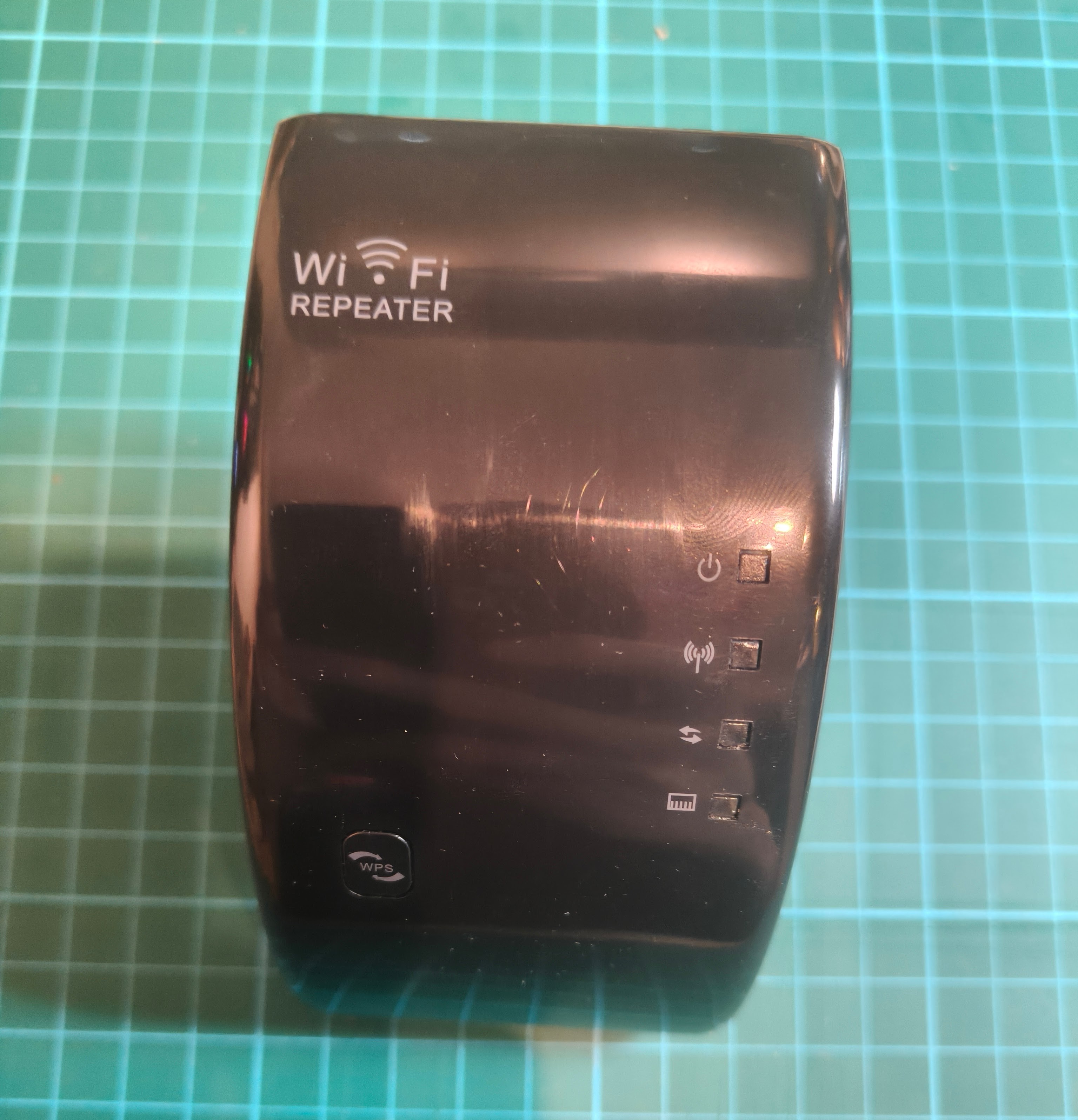
In this series, I will be documenting my journey of trying to reverse engineer a random (cheap) WiFi repeater. A family member was about to discard this device before I took it, thinking it would be interesting to see what I can find.
Since the device was about to become e-waste, I received it with no documentation or user instructions. However, a quick search showed me that I was probably dealing with one of those generic brandless WiFi range extension devices. This particular device was probably purchased from Taobao quite a while back.
Device teardown
With the help of a flat head screwdriver prying open the plastic shells, the internal PCB can be revealed. 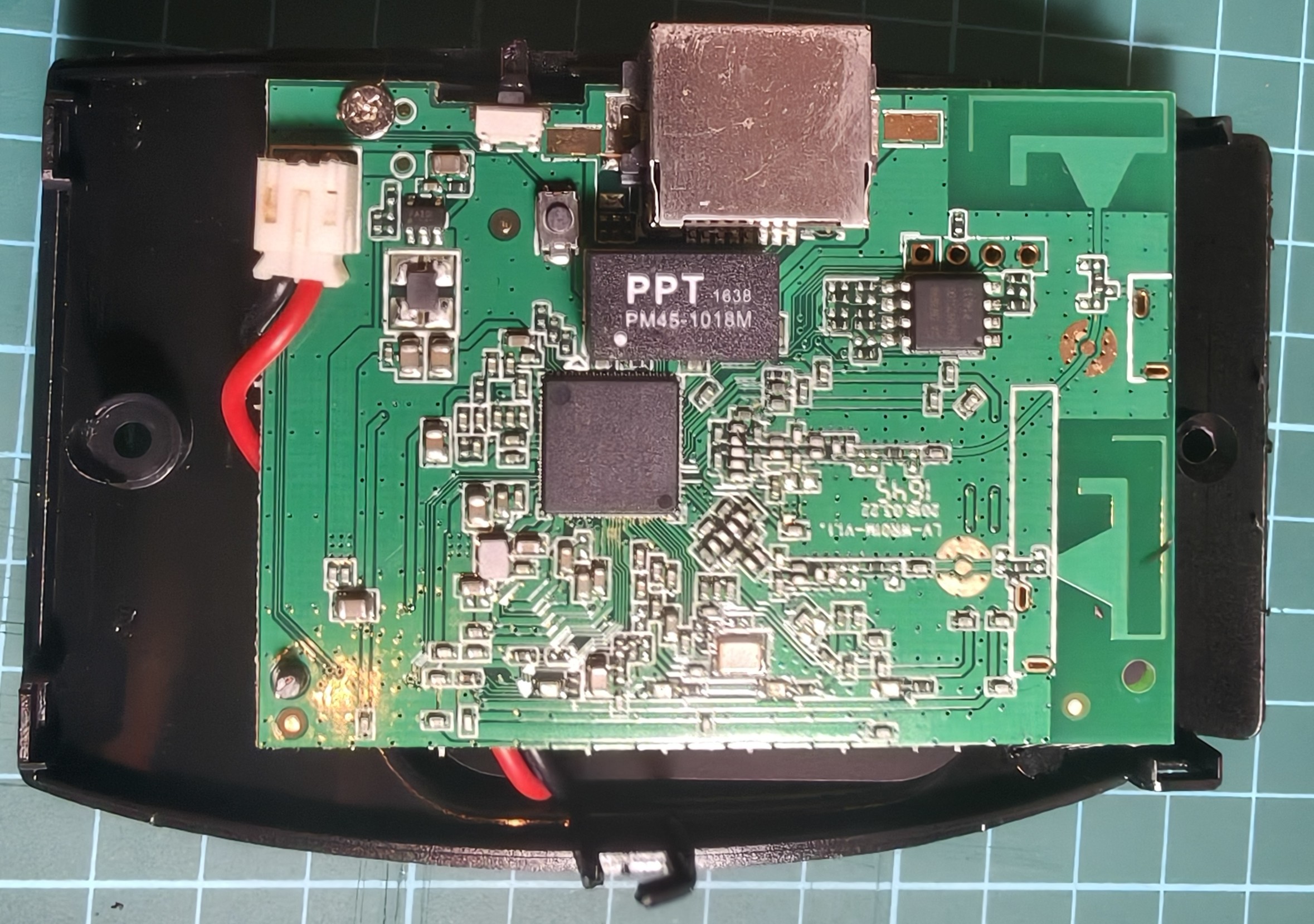
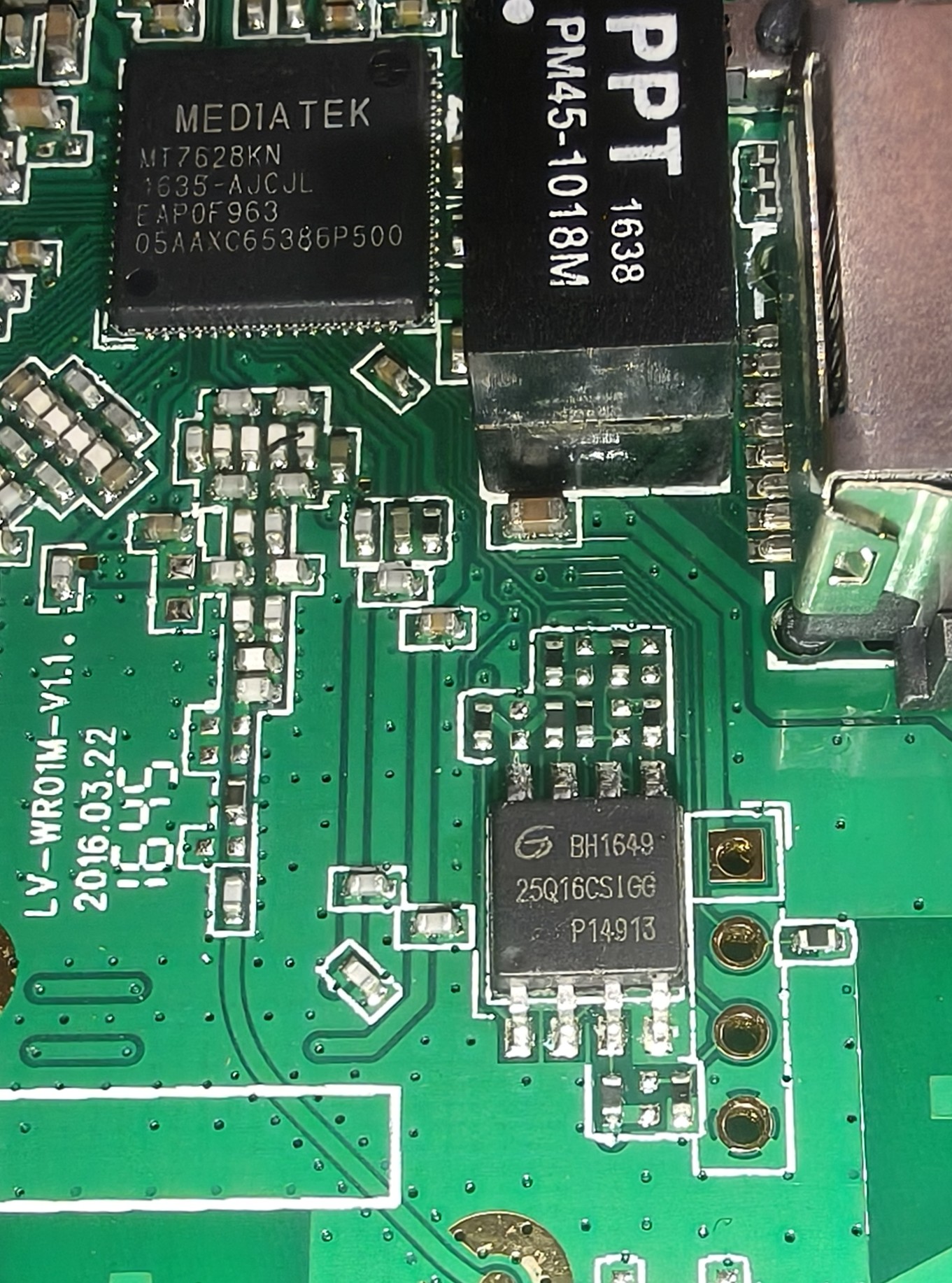
The PCB isn’t very huge, but it contains some features of interest. In particular, a processor unit (black square), flash memory chip (rectangle on the top right with 8 pins) and (possibly?) UART debugging port can be found. There is also a RJ45 port near the top of the PCB (big silver thing).
The path of least resistance
While I could immediately go with trying to dump the data stored on the flash memory, I opted to take the easiest route first — trying to interface with the board through the UART port. My (very limited) experience in reverse engineering has taught me the path of least resistance often gives you the highest effort to impact ratio (low effort but potentially high impact).
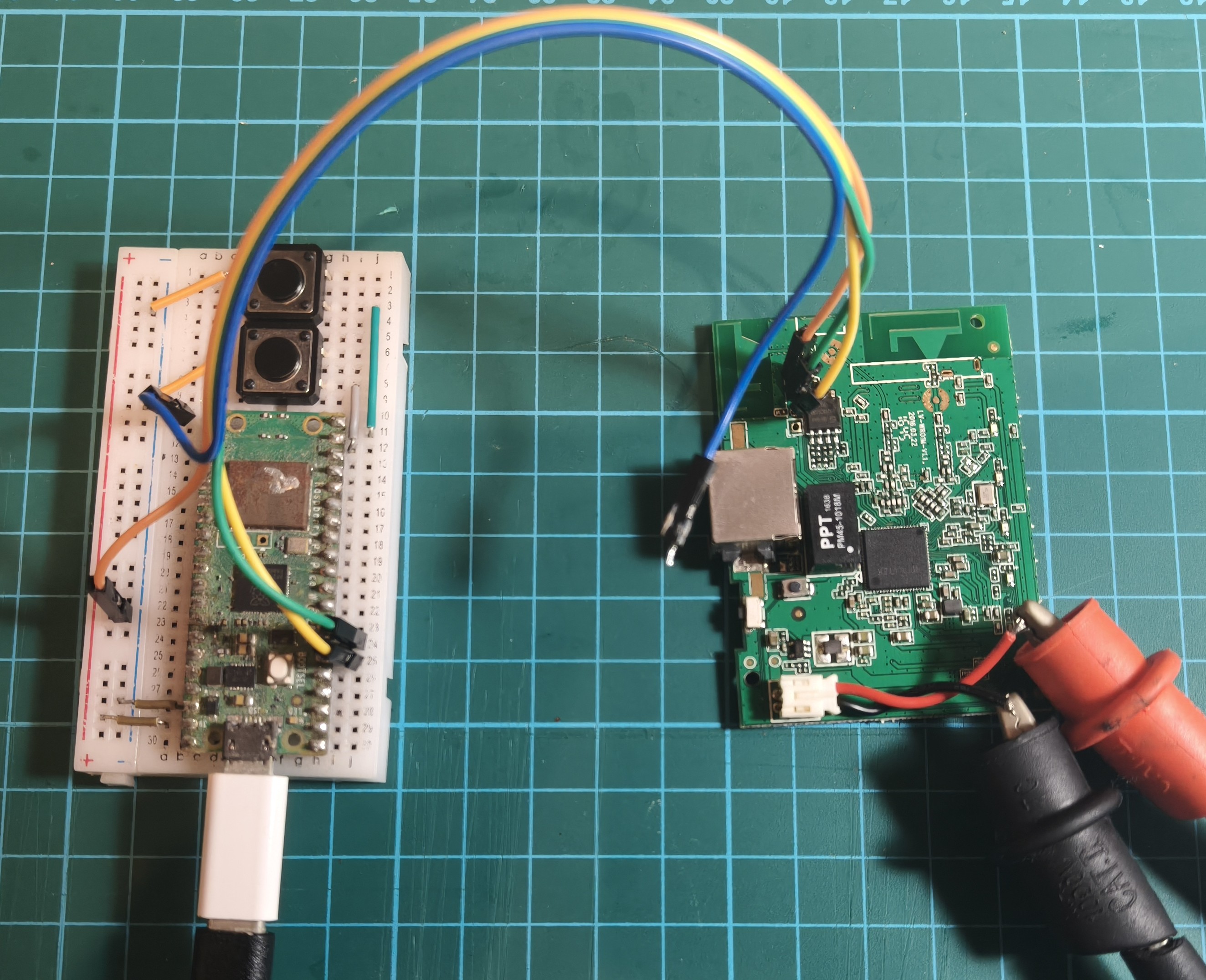
Anyway, to interface with the board, I will be using a raspberry pi pico (RP2040 based MCU) with some firmware to enable it to act as a UART to USB bridge, essentially converting data transmitted using UART to serial USB, allowing my computer to understand the data through a serial interface.
The path of least resistance, literally
Before we can connect wires to the board though, we need to figure out the purpose of each hole on the UART port. Since I only have a multimeter, I resorted to using a pretty cool method of determining the purpose of the holes.
- Connect multimeter negative to a known ground point on the board (tip: the outer metal shells of connector ports are usually grounded, in this case I connected my negative lead to the metal shell of the RJ45 port)
- Power on the board (in this case I powered the board with 5V, an educated guess since I don’t know the correct voltage)
- Touch the positive to each of the holes and observe the reading on the multimeter
- If the voltage is the same as that supplied, it is VCC
- If the voltage fluctuates up and down, it is likely the device’s TX (note: we are making an assumption here that data is actively being transmitted)
- If the voltage stays at zero (the path of least resistance), it can either be RX or GND (note: I haven’t found a way to differentiate between the two, so I’m still resorting to trial and error)
Now, at least the device’s TX pin is known so its output can be read! After some trial and error swapping the connection between the jumper wires and the holes, the RX and GND pins can be correctly identified. It turns out the order is ■ ● ● ● -> 5V, board RX, board TX, GND, which I got to learn later is actually quite a common layout.
Now back to the software realm
Hopping over to my computer, I can now read the output from the board using the serial terminal. On powering the device, a flurry of text is observed. Strangely enough, the device seems not be able to properly boot into its firmware and seems to be stuck in some sort of loop between in bootloader menu and attempting to execute the target binary (perhaps that’s why it was being discarded?).
1
2
3
4
5
6
7
8
9
10
11
12
13
14
15
16
17
18
19
20
21
22
23
24
25
26
27
28
29
30
============================================
Ralink UBoot Version: 4.3.0.0
--------------------------------------------
ASIC 7628_MP (Port5<->None)
DRAM component: 64 Mbits DDR, width 16
DRAM bus: 16 bit
Total memory: 8 MBytes
Flash component: SPI Flash
Date:Aug  7 2016  Time:16:01:36
============================================

Please choose the operation:
   1: Load system code to SDRAM via TFTP.
   2: Load system code then write to Flash via TFTP.
   3: Boot system code via Flash (default).
   4: Entr boot command line interface.
   7: Load Boot Loader code then write to Flash via Serial.
   9: Load Boot Loader code then write to Flash via TFTP.

 Normal Mode!

3: System Boot system code via Flash.
## Booting image at bc050000 ...
   Image Name:   zxrouter
   Image Type:   MIPS Linux Standalone Program (uncompressed)
   Data Size:    881564 Bytes = 860.9 kB
   Load Address: 80500000
   Entry Point:  80500000
   Verifying Checksum ... OK
OK
Interestingly, though, it can also be seen that in the booloader menu, it seems to give us a choice to enter a command line interface. Thankfully, since we are able to send data to the board too, we can attempt to interrupt the normal boot sequence. I did so by spamming sending 4 to the device when powering on. Once in, I tried standard shell commands (like ls, whoami, pwd) but they all didn’t seem to work, suggesting we were not working with a standard OS.
Entering help however, worked! A list of available commands are displayed upon entering help.
1
2
3
4
5
6
7
8
9
10
11
12
13
14
15
16
17
18
19
20
help
?       - alias for 'help'
bootm   - boot application image from memory
cp      - memory copy
erase   - erase SPI FLASH memory
go      - start application at address 'addr'
help    - print online help
loadb   - load binary file over serial line (kermit mode)
md      - memory display
mdio   - Ralink PHY register R/W command !!
mm      - memory modify (auto-incrementing)
nm      - memory modify (constant address)
printenv- print environment variables
reset   - Perform RESET of the CPU
rf      - read/write rf register
saveenv - save environment variables to persistent storage
setenv  - set environment variables
spi     - spi command
tftpboot- boot image via network using TFTP protocol
version - print monitor version
I managed to look at the environment variables.
1
2
3
4
5
6
7
8
9
10
11
12
13
bootcmd=tftp
bootdelay=2
baudrate=57600
ethaddr="00:AA:BB:CC:DD:10"
filesize=d73a8
fileaddr=80A00000
ipaddr=10.10.10.123
serverip=10.10.10.3
autostart=no
bootfile=eCos_MT7628K_20161224_upgrade.img
stdin=serial
stdout=serial
stderr=serial
The path of least resistance pays off
Initially, I was worried that I would have to dump the firmware by connecting a SOIC-8 clip to the flash memory chip. I tried this previously and it yielded terrible results (i.e. it didn’t work and was incredibly frustrating), so I really wanted to avoid doing it.
But miraculously, the CLI gives us an easy way to read the flash memory! I proceeded to try and dump the target binary using the command device-shell# md.b bc050000 d739c (offsets and lengths obtained from boot logs). Since we were dumping through UART, it was pretty slow as the device basically started printing out the bytes in a hexdump format. I stored the text output and used a Python script to convert it into binary data which we can then analyse using more common reverse engineering tools.
What next
I’m currently working on figuring out the structure of the carved file and trying to figure out how to start reverse engineering it. It will probably take me quite some time but when it’s done, the second post in this series will be up!